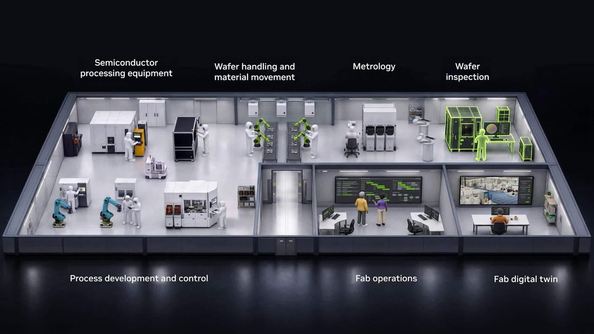
Semiconductor equipment manufacturers and software developers are integrating NVIDIA accelerated computing and physics-based AI to speed up semiconductor fabrication workflows. The tools target complex process modeling, physical trials reduction, and fab engineering optimization.
Software maker COMSOL and simulation provider Applied Materials integrated the NVIDIA cuDSS library to accelerate multiphysics and materials simulation workloads by up to 10x. Additionally, Applied Materials deployed the NVIDIA PhysicsNeMo framework to speed up topography simulations up to 35x, while Lam Research demonstrated millisecond-level plasma behavior predictions using the same physics-informed neural network framework.
In computational lithography, Siemens integrated NVIDIA cuLitho into its Calibre software suite, reporting up to 17x acceleration on simulation workloads. The performance gains enable engineers to test significantly more process variations virtually, improving yield optimization and accelerating time-to-market for next-generation silicon production.
Why it matters
Physics-informed AI models drastically reduce the computational time and cost required to simulate advanced semiconductor fab operations.
Computational lithography and plasma modeling tools enable faster design cycles and higher yield optimization for next-gen silicon.
Integration of accelerated math libraries like cuDSS cements GPU acceleration as standard infrastructure across electronic design automation.
Source: blogs.nvidia.com